
The paper “Imaging junctions in two-dimensional semiconductor nanosheet networks” has just been published in npj 2D Materials & Applications. The research was led at the Institute of Physics Belgrade (IPB) by Dr. Jelena Pešić, a member of the HIP-2D-QM team supported through Horizon Europe, together with collaborators from Montanuniversität Leoben (Austria), Trinity College Dublin (Ireland), and Universidade NOVA de Lisboa (Portugal).
Instead of focusing only on morphology or conventional microscopy, this study addresses one of the biggest open questions for scalable 2D electronics: how does charge actually travel through solution-processed 2D material films in real devices?
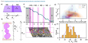
To answer this, it used in-operando Kelvin probe force microscopy (KPFM) to directly visualize potential drops across individual MoS₂ nanosheets, and crucially - heir junctions inside functioning transistor structures. By combining these measurements with Y-function analysis and network modelling, the researchers showed that junctions between nanosheets dominate overall resistance and play a key role in shaping device performance.
These insights strongly support the vision of the HIP-2D-QM Horizon Europe project, which aims to develop advanced quantum and functional materials, including scalable 2D systems for future technologies.
The full open-access article is available in npj 2D Materials & Applications.